Three-dimensional imaging of carbon nanotubes under scanning electron microscopy
Measuring the dispersion of carbon nanotubes (CNTs) embedded in a polymer matrix is crucial in understanding the process-structure-property relationships of CNT nanocomposites. Scanning electron microscopy (SEM) is normally used for this two-dimensional (2D) surface imaging. Now, reporting in Nanotechnology, researchers show that quantitative three-dimensional (3D) imaging of CNTs embedded in a polyimide matrix can be conducted non-destructively under SEM.
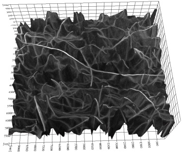
3D SEM imaging of 0.5% CNT-polyimide composites
The contrast mechanism of CNTs embedded in a polymer matrix is studied through extensive experiments. Surface and cross-sectional SEM imaging, beam-induced current measurement, focussed ion beam milling, and Monte Carlo simulations are used. In particular, a concept of third crossover energy is proposed to account for the high resolution subsurface imaging of CNTs achieved by a high energy electron beam. This technique can help establish SEM as a practical method to provide quantitative 3D information on CNT dispersions in polymer composites. Additionally, it has an imaging depth of up to 1 µm.
Improved throughput
Compared to the team previous work on subsurface imaging based on electric force microscopy (Minhua Zhao et al. 2010), the current technique has a much higher throughput and more quantitative depth information. Yet, the application of these techniques is not limited to CNT-polymer composites. They are generally applicable to the subsurface imaging of conducting nanostructures embedded in a dielectric matrix e.g. graphene polymer composites or integrated circuit conductors covered by a dielectric layer. This may have significant implications in non-destructive imaging of silicon nanostructures embedded in silicon oxide for single electron transistors or high resolution SEM overlay metrology.
Improving resolution
One of the challenges for subsurface imaging under SEM is that spatial resolution at a deeper location is reduced due to the scattering of electrons in materials. The team are continuing their efforts in this field and have stronger evidence regarding the existence of ‘third crossover energy . Stay tuned.